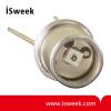
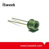
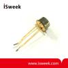
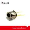
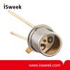
Concentrator Lens SiC UV Photodiode - SG01D-5Lens
• Broadband UVA+UVB+UVC, PTB reported high chip stability, for fame detection
• Radiation sensitive area A = 11,0 mm2
• TO5 hermetically sealed metal housing with concentrator lens, 1 isolated pin and 1 case pin
• 10µW/cm2 peak radiation results a current of approx. 350 nA
• Dark Current: 1.7 fA
• Capacitance: 125 pF
• Responsivity Range: 221 … 358 nm
- Quantity:
- - +
Product Specification
SG01D-5LENS
Concentrator lens SiC based UV photodiode Avirtual = 11.0 mm2
◆ SG01D-5Lens SiC UV Photodiode General features
Properties of the SG01D-5LENS UV photodiode
• Broadband UVA+UVB+UVC, PTB reported high chip stability, for fame detection
• Radiation sensitive area A = 11.0 mm2
• TO5 hermetically sealed metal housing with concentrator lens, 1 isolated pin and 1 case pin
• 10µW/cm2 peak radiation results a current of approx. 350 nA
About the material Silicon Carbide (SiC)
SiC provides the unique property of extreme radiation hardness,
near-perfect visible blindness, low dark current, high speed and low
noise. These features make SiC the best available material for
visible blind semiconductor UV detectors. The SiC detectors can be
permanently operated at up to 170°C (338°F). The temperature
coeffcient of signal (responsivity) is also low, < 0.1%/K.
Because of the low noise (dark current in the fA range), very low
UV radiation intensities can be measured reliably.
Options
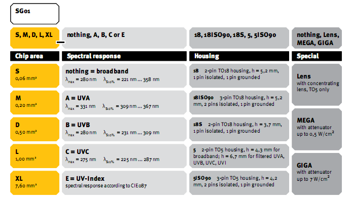
SiC photodiodes are available with seven different active chip areas
from 0.06 mm2 up to 36 mm2 Standard version is broadband UVA-UVB-UVC.
Four fltered versions lead to a tighter sensitivity range. All
photodiodes have a hermetically sealed metal housing (TO type), either
a 5.5 mm diameter TO18 housing or a 9.2 mm TO5 housing. Further
option is either a 2 pin header (1 isolated, 1 grounded) or a 3 pin
header (2 isolated, 1 grounded).
◆ SG01D-5Lens SiC UV Photodiode Nomenclature
◆ SG01D-5Lens SiC UV Photodiode Specifications
| Parameter | Symbol | Value | Unit |
|
|
|
|
|
| Spectral Characteristics |
|
|
|
| Typical Responsivity at Peak Wavelength | Smax | 0.130 | AW-1 |
| Wavelength of max. Spectral Responsivity | λmax | 280 | nm |
| Responsivity Range (S=0.1*Smax) | – | 221 … 358 | nm |
| Visible Blindness (Smax/S>405nm) | VB | > 1010 | – |
|
|
|
|
|
| General Characteristics (T=25°C) |
|
|
|
| Sensitive Area (chip size = 0.50 mm2) | A | 11.0 | mm2 |
| Dark Current (1V reverse bias) | Id | 1.7 | fA |
| Capacitance | C | 125 | pF |
| Short Circuit (10µW/cm2 at peak) | Io | 350 | nA |
| Temperature Coefficient | Tc | < 0.1 | %/K |
|
|
|
|
|
| Maximum Ratings |
|
|
|
| Operating Temperature | Topt | -55 … +170 | °C |
| Storage Temperature | Tstor | -55 … +170 | °C |
| Soldering Temperature (3s) | Tsold | 260 | °C |
| Reverse Voltage | VRmax | 20 | V |
If you cannot find what you want, you can entrust OFweek to source for you. Just click:
Sourcing Service


